Circuit board printer

© Nano Dimension

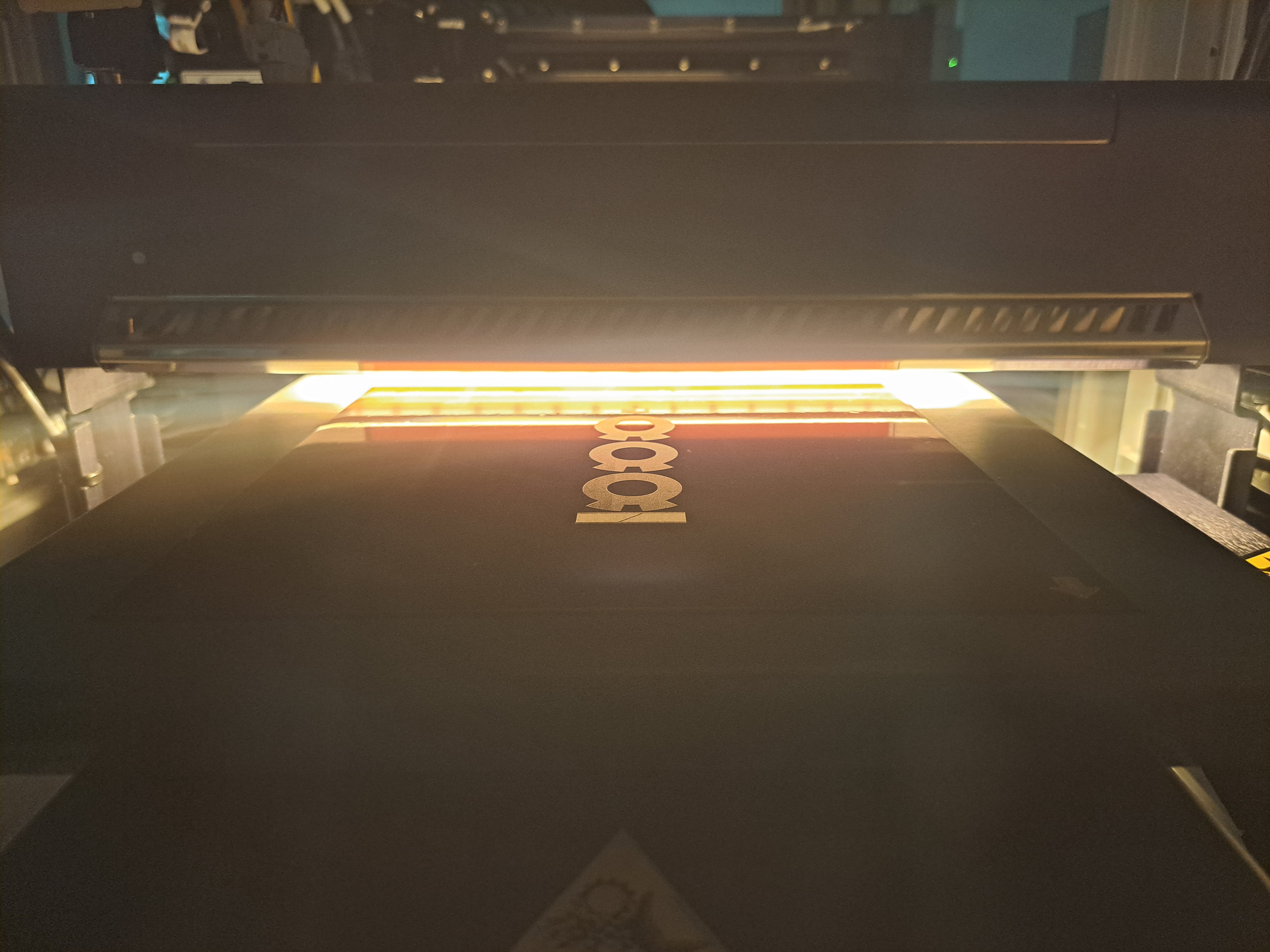
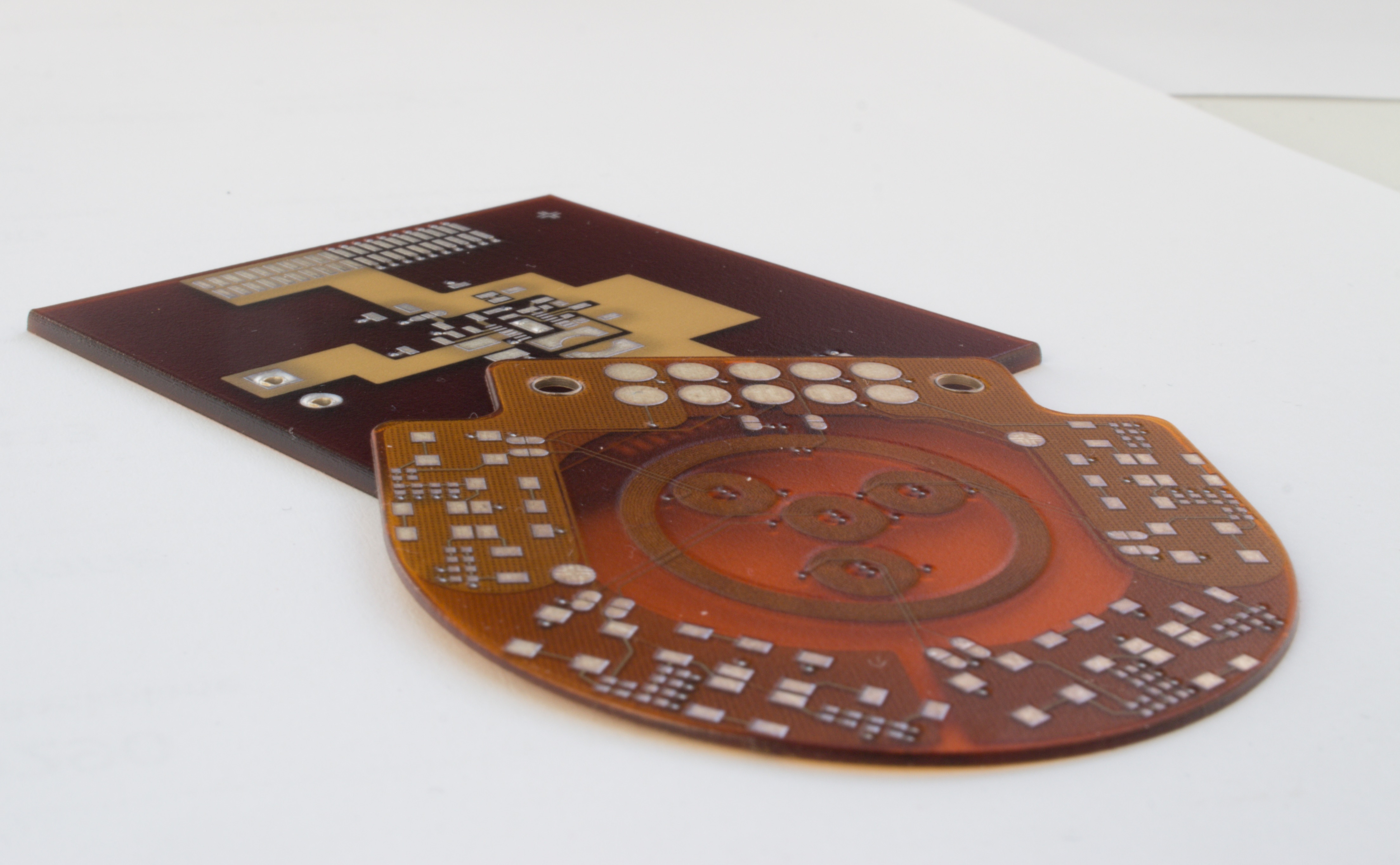
Modern sensor and electronics development requires the use of innovative manufacturing technologies. This is why the Fraunhofer Center for Sensor Intelligence ZSI relies on novel processes such as 3D printed circuit board printing.

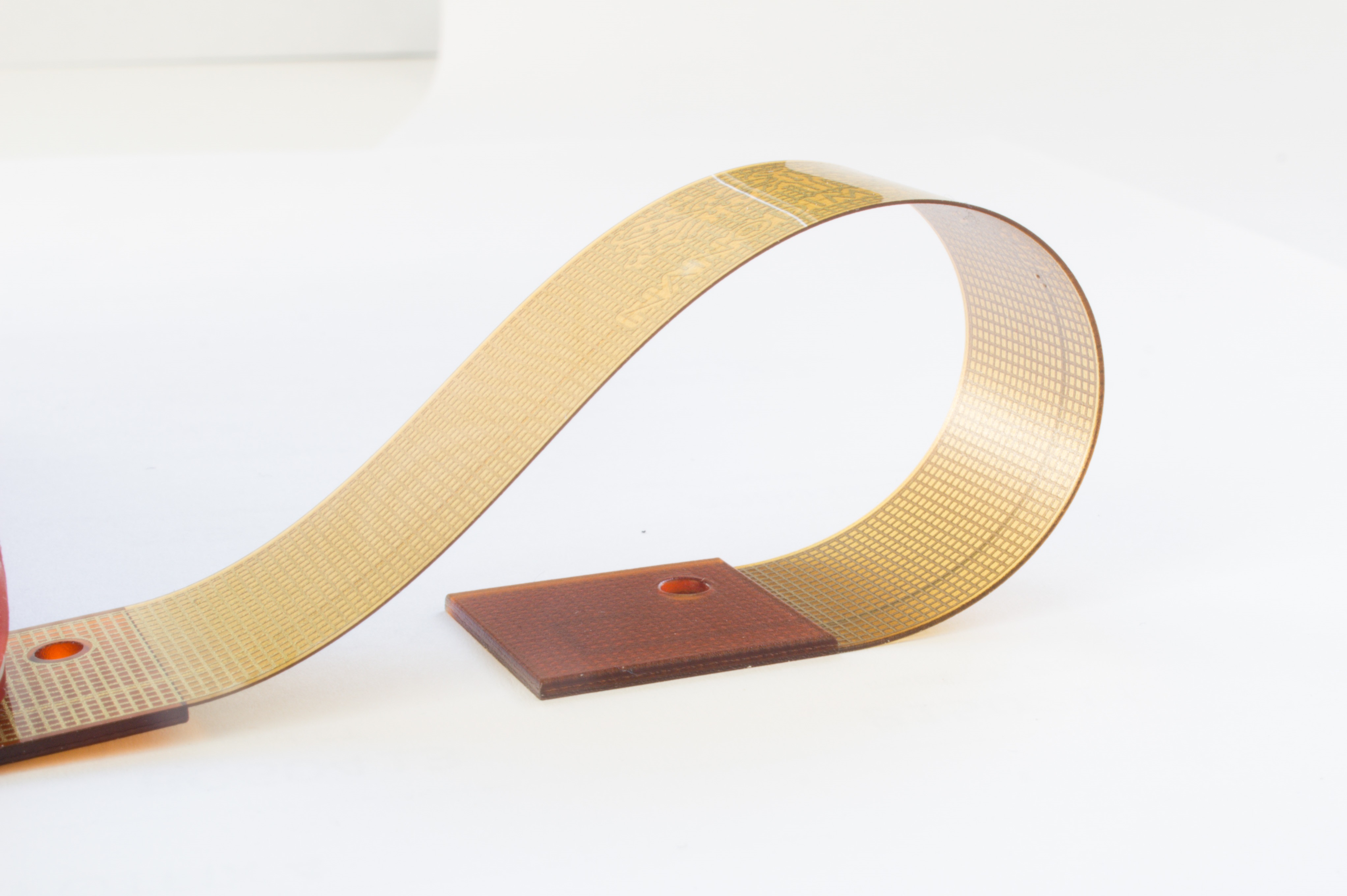
This type of production opens up a multitude of new possibilities for the scientists at the Fraunhofer ZSI, as the classic layer structure familiar from conventionally manufactured printed circuit boards is no longer required.

Instead, the process enables the three-dimensional design of circuit boards, antennas and sensors within the technological and technical limits of the process and the production plant.

The system used relies on dual inkjet printing. Two different materials, an epoxy resin as a dielectric and an ink mixed with silver nanoparticles, are used as a conductive material for conductor path structures. 

Conductor track structures with a minimum width of up to 75 µm and a minimum thickness of 17 µm are technically possible. The installation space of 160 mm x 160 mm x 5 mm can be fully utilized in three dimensions.

PCBs

© Fraunhofer IZFP

The manufacturing process enables fast and uncomplicated production of PCB prototypes in different variants and without significant waiting times.

Classic PCB structures in formats such as ODB++ or Gerber can be produced as well as completely free-form trace structures without a fixed layer structure, which offers an enormous advantage in terms of signal integrity, especially in the area of higher frequencies.

This means that PCBs can be optimized, adapted and produced down to the smallest detail for the respective application and requirement.

  1. Replacing vias with flowing transitions (HF applications)
  2. Embedding components (increasing the packing density)
  3. Printing components (coils, capacitors, resistors)
  4. Transitions between rigid and flexible areas.

Sensor technology

© Fraunhofer IZFP

This technology also gives us an enormous advantage in the area of sensor development and production.

Sensors and sensor systems can be adapted directly to the geometry to be tested, such as double-curved surfaces. On the other hand, inductive sensors, for example, can also be designed as freeforms in such a way that they are optimally adapted to the respective requirements in terms of their field propagation and associated sensitivity.

Furthermore, the sensors developed in this way can be supplemented directly with appropriate electronics, which has a positive effect on their signal quality.